Taiyo Nippon Sanso will be Exhibiting at the 63rd Electronic Materials Conference, June 23rd-25th, 2021
Click for Details
Nippon Sanso Announces Strategic Alliance with 3D Printing Corporation K.K.
Taiyo Nippon Sanso Corporation (“Nippon Sanso”) hereby announces that it has
achieved strategic alliance with 3D Printing Corporation K.K. (“3DPC”) in
Japan.
1. Overview on the Strategic Alliance
Nippon Sanso has been promoting and expanding 3D Printing business (Additive
Manufacturing “AM”). Nippon Sanso has launched differentiated products and
enhanced technical expertise thru partnership in the AM industry.
3DPC has founded in 2016 as an AM-related venture company in Japan and aim
to build a new 3D Printing based supply chain including into various products
to achieve its vision of revitalizing Japan manufacturing with 3D printing
manufacturing technologies.
The strategic alliance enables not only Nippon Sanso to introduce 3DPC’s products and
service into the broad network of Nippon Sanso but also to build business and technical
synergy with our metal 3D printer and gas solution system.
Note (*): DFAM
DFAM is a general term of design concept and tools for making the most
of AM technologies. e.g. optimization of design for light weighting parts
2. Overview of 3DPC
Name : 3D Printing Corporation K.K.
HQ and plant : LVP1-101,75-1, Onocho, Tsurumi,
Yokohama, Kanagawa, Japan
Establishment : 2016
Representative : Alexander De Vore
Taiyo Nippon Sanso Corporation
Successful metalorganic vapor phase epitaxy of β-gallium oxide crystals
Tokyo University of Agriculture and Technology
Gas-Phase Growth Ltd.
Taiyo Nippon Sanso Corporation
Accelerating the realization of a carbon-free society through next-generation power devices
In collaboration with Dr. Hideaki Machida (President) and Dr. Masato Ishikawa of Gas-Phase Growth Ltd. and Mr. Kazutada Ikenaga of Taiyo Nippon Sanso Corporation (President: Kenji Nagata), Professor Yoshinao Kumagai and Assistant Professor Ken Goto of Division of Applied Chemistry, Institute of Engineering, Tokyo University of Agriculture and Technology (President: Kazuhiro Chiba), have revealed the chemical reaction mechanism of vapor phase growth of β-gallium oxide (β-Ga2O3) crystals (Note 1), which are attracting attention as materials for next-generation power devices with high energy-saving effects. The metalorganic vapor phase epitaxy (MOVPE) method (Note 2) was used to demonstrate the growth of high-purity β-Ga2O3 crystals under optimal growth conditions. These results hold promise to lead to the development of mass-production MOVPE equipment for β-Ga2O3 devices, and the practical application of β-Ga2O3 power devices for a decarbonization society.
Please refer to the Japanese Journal of Applied Physics (abbreviated as JJAP) on March 29 for the results of this study.
Title: Thermodynamic and experimental studies of β-Ga2O3 growth by metalorganic vapor phase epitaxy
URL: https://doi.org/10.35848/1347-4065/abec9d
(Note 1) β-gallium oxide (β-Ga2O3)
An oxide semiconductor crystal in which gallium (Ga) and oxygen (O) atoms are combined in a stoichiometric ratio of 2 : 3. Its band gap is about 4.5 eV, which is larger than that of Si (1.1 eV), 4H-SiC (3.3 eV) and GaN (3.4 eV).
(Note 2) Metalorganic Vapor Phase Epitaxy (MOVPE)
A method of crystal growth using organometallic compound gases as raw material. The film thickness can be controlled with a precision of one atomic layer, and it is widely used as a method for fabricating compound semiconductor devices that require nanometer-order* structure design. It is widely used in the fabrication of nitride semiconductor light-emitting devices and high-speed transistors, but has not been investigated in oxide crystal growth due to the high reactivity of oxygen with organometallic compounds.
* 1 nanometre is one billionth of a metre
◆Research-related inquiry
Tokyo University of Agriculture and Technology
Division of Applied Chemistry, Institute of Engineering
Professor Yoshinao Kumagai
E-mail:[email protected]
Gas-Phase Growth Ltd.
Hideaki Machida, President
E-mail:[email protected]
Taiyo Nippon Sanso Corporation
Compound Semiconductor EquipmentDept., Innovation Unit
Kazutada Ikenaga
E-mail:[email protected]
Taiyo Nippon Sanso MOCVD equipment division receiving Industry Award
Taiyo Nippon Sanso MOCVD equipment division receiving the Industry Award from The Japan Society of Vacuum and Surface Science
Taiyo Nippon Sanso Corporation (“Nippon Sanso”) (President:Kenji Nagata) announces that its MOCVD
equipment division for advanced GaN and AlN devices has received the 2020 Industry Award from
The Japan Society of Vacuum and Surface Science.
This award is presented annually by The Japan Society of Vacuum and Surface Science to
recognize significant contributions to the advancement and development of the surface and vacuum
science-related industries.
<Taiyo Nippon Sanso MOCVD Equipment Division>
Nippon Sanso has been developing MOCVD (Metal Organic Chemical Vapor Deposition) compound
semiconductor production equipment since 1983, and has delivered more than 500 MOCVD
equipment sets to manufacturers and research institutions in Japan and abroad.
In 2015, Nippon Sanso developed the SR4000HT reactor model for high Al content AlGaN ultraviolet
(UV) light-emitting devices. The SR4000HT allows for AlGaN film deposition at a high
temperature (greater than 1300 °C). Processes for UVLED epi-wafers with high luminous
efficiency have demonstrated.
In 2012 Nippon Sanso introduced the UR26K reactor model, a large-scale mass production platform that
can process 8-inch substrates. High performance mass production of GaN HEMTs on 8-inch Si
substrates has been demonstrated. The UR series reactors optimize film properties and productivity
by reducing the operating time and supporting cleaning technology for reactor components.
Nippon Sanso will continue will contribute to promote environmental and energy conservation initiatives
in the industry by introducing new technologies and products.
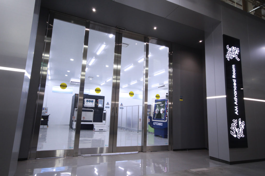
Opening of Additive Manufacturing Advanced Room
Taiyo Nippon Sanso Corporation (“Nippon Sanso”) (President: Kenji Nagata) hereby announces the opening of “AM Advanced Room” as a research & development base of additive manufacturing technology.
1. Background
Nippon Sanso has been focusing on Additive Manufacturing (“AM”) technology as one of the core field of Industry Revolution 4.0. AM has been adopted to global manufacturing industry as the technology is expected to contribute to a sustainable society through supply chain innovation. Based on the innovation strategy outlined in “Ortus Stage 2″—the mid-term management plan of Nippon Sanso Holdings—Nippon Sanso is dedicated to metal AM business as a priority area.
Nippon Sanso recently openedan AM Advanced Room at its Yamanashi Laboratory as a core hubforthe research & development of AM technologies. The purpose of the new hubis to provide total solutionsfor various industries aiming to take advantage of metal AM. In AM Advanced Room,Sapphire®printers by VELO3D—as next generation PBF platform, LENS®by Optomec,and 3DPro®products, which utilize proprietarygas technologyof Nippon Sanso group.In addition, Nippon Sanso will actively address to global market withmore innovative modeling processes. By delivering the most advanced solutions, Nippon Sanso will be able to significantly contribute to corporate sustainability.
2. “AM Advanced Room” Overview
Place: Taiyo Nippon Sanso Yamanashi Laboratory
Established: October of 2020
Objectives: Development of core AM technologies, demonstrations, total-solution creation, customer support, etc.